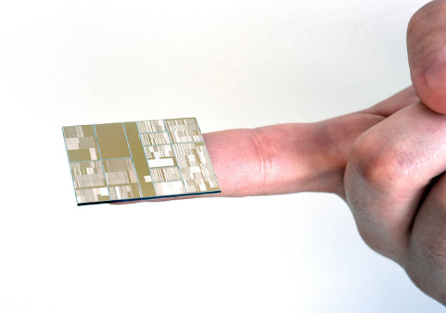
IBM has taken the technology industry with surprise through its announcement of successfully developing working versions of ultradense computer chips. These chips are said to possess four times the capacity of today’s most powerful chips.
This announcement was essentially made on behalf of an international consortium led by IBM. IBM has invested $3 billion in an exclusive private public partnership in New York’s Hudson Valley with New York State, Samsung, GlobalFoundries and equipment vendors to manufacture advanced computer chips.
New Generation Of Chip In Development
It should be noted that each generation of chip is defined by the minimum size of fundamental components, which play role in switch current at nanosecond intervals. In modern times technology industry is actively working towards making a commercial transition from 14 nanometer to 10 nanometer manufacturing. Each generation helps in achieving 50 per cent reduction in the amount of area required for circuitry. IBM has affirmed its new chip which is still in research phase will be based on the shirking the area of semiconductor as much as possible by 2018.
IBM currently has working samples of chips with just seven nanometer transistors. It has been able to develop such sizes due to use of advanced silicon-gremanium instead of relying on pure silicon in key regions of chip. This material has made it possible to develop faster transistor switching with low power requirements, which is an added advantage. Given the smaller size of the transistors, it is highly possible to build microprocessors with not more than 20 billion transistors.
IBM Brings Focus Back On Itself As Revolutionary Chip Manufacturer
IBM has already shed a certain amount of its computer and semiconductor manufacturing capacity in the recent past. But this announcement shows that IBM is still interested in backing the technology manufacturing base with its efficient research facilities. Rather than being the horse power in building and providing chips to the companies it will act as a pioneer in unearthing advanced technological solutions for others. IBM will have to grapple with shift to use extreme ultraviolet (EUV) light for etching patterns on the chips at a resolution which approaches the diameter of an individual atom.
IBM will be licensing the technology to a variety of manufactures and most importantly, GlobalFoundries which is owned by the Emirate of Abu Dhabi will be making these chips for some big companies which includes, Qualcomm, Broadcom and others. It is yet to been whether semiconductor industry thinks on using silicon-gremanium as the best option or not.
IBM Refuses To Confirm Commercial Manufacturing
IBM has simply declined whether it will begin commercial manufacturing of this technology or not. Another ambitious company named Taiwan Semiconductor Manufacturing Company had given green lights to its plans to begin production of seven nanometer chips in 2017.
Given the precision required for using EUV light to keep the high capacity usage of chips optimum might be a concern in the commercial manufacturing operations. The goal of IBM here is to create next generation circuits, which offer higher capacity with reduced area, and most probably with current advancements and right amount of further research this technology will be introduced next year.


No comments:
Post a Comment